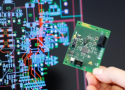
®DenciTec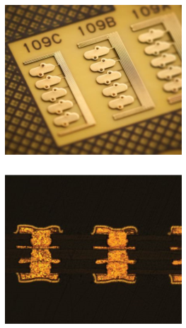
Combining PCB production processes
Swiss engineered technology
-
MiniaturizationLines/spaces down to 25/25 μm (1 mil) with20 µm Cu thicknessSignificantly higher level of integrationFor example: more volume for energy supply, batteries, etc.
-
Higher packaging densitiesMore design options
-
More functionalitySmarter products with more features
-
Lower costs compared to other technologiesEconomic